A return path in a PCB refers to the low-impedance path through which current flows back to the source after passing through a circuit component.
The return current typically traverses through ground planes or adjacent conductive layers to complete the circuit loop.
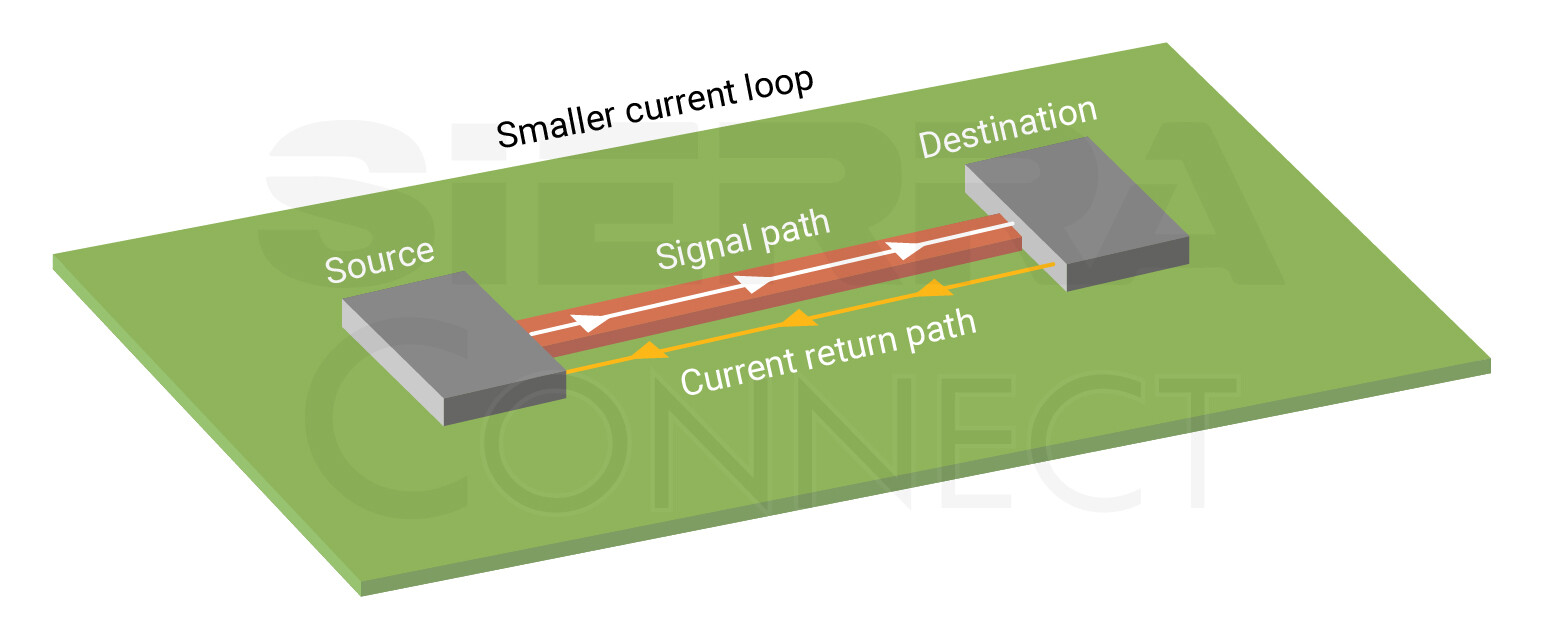
If the return path is poorly designed, return currents may detour, increasing the loop area and making the circuit susceptible to noise, crosstalk, or EMI, especially in high-speed digital or analog circuit designs.
Factors affecting return path quality:
- Reference plane continuity: Gaps, splits, or voids in ground/power planes might introduce impedance discontinuities and parasitic effects.
- Via transitions: When a signal changes layers, parasitic inductance might increase.
Trace routing: Long, meandering traces or routes crossing plane splits disrupt return current flow. - Layer arrangement: Poorly planned buildups without adjacent ground planes increase loop inductance.
- Dielectric material: The dielectric constant (Dk) and thickness of the substrate between signal and return paths increase the capacitance and impedance of the return path.
Design guidelines for optimizing return path:
- Always route signal traces over a solid, continuous reference plane (typically ground).
- Avoid splits and gaps in ground planes beneath critical signal traces; if unavoidable, provide a stitching capacitor for current continuity.
- Minimize the distance between signal and return paths to reduce signal loop area and noise coupling.
- Use stitching vias around high-speed/RF traces and at layer transitions to maintain low-impedance return current continuity, as these are closely spaced vias that connect ground planes across PCB layers. The recommended spacing between the stitching vias is λ/20 to λ/10, where λ is the operating wavelength.
- Employ wide, low-impedance ground traces in designs without dedicated ground planes, and keep them as close as possible to signal traces.
- Avoid having two adjacent signal layers; separate them by at least one dielectric layer.
- Keep decoupling capacitors close to IC power pins to provide localized return paths for high-frequency currents.
- Maintain consistent spacing and symmetry between the differential traces to minimize common-mode noise, as most of the return current from one trace couples directly into the other due to tight electromagnetic field coupling.
A well-designed return path is essential for robust PCB performance. Ignoring return path principles can result in unwanted emissions, degraded signals, and unreliable operation in high-speed or sensitive circuits.