
PCB vias are plated holes that establish an electrical connection among different layers of a PCB. Vias enable the miniaturization and complexity that advanced electronic designs demand, allowing signals and power to navigate through dense circuit topologies.
Functionality of vias: what do they really do?
Vias act as essential connectors, enabling electrical signals or power to transition between different layers of a printed board.
Without vias, signal routing would be restricted to a single copper layer, severely limiting board density and functionality. They connect components to internal power planes, link signal traces across layers, and provide heat dissipation paths for thermal management.
Vias influence several key performance characteristics:
- Signal integrity (SI): Poorly placed or stubby vias can cause reflections, impedance mismatches, and signal degradation at high frequencies.
- Power integrity (PI): Vias serve as power delivery paths and should be designed to handle the desired current and reduce IR drop.
- Thermal management: Thermal vias dissipate heat from power components to internal or bottom layers with ground planes.
From a mechanical perspective, vias must withstand thermal cycling, mechanical stresses, and fabrication tolerances. Poorly designed vias can result in barrel cracking, plating voids, or delamination, especially in class 3 applications.
Common via types
There are four common via types in PCBs, each with its own manufacturing process, electrical behavior, and typical uses:
- Through-hole vias
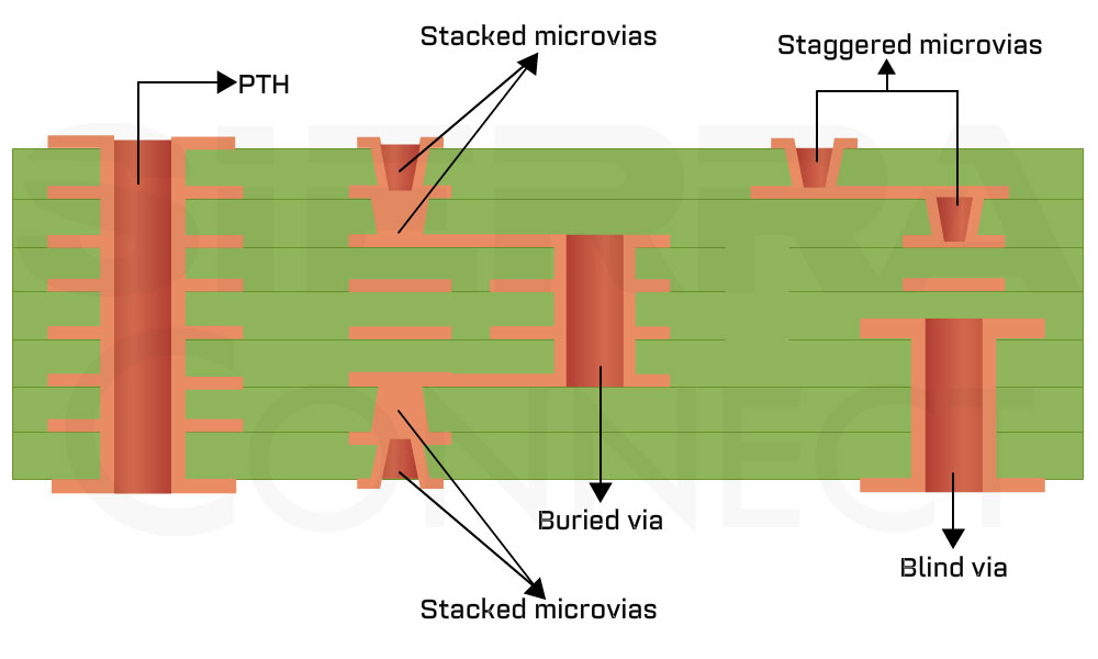
These vias connect all layers from the top to the bottom. Through-hole vias are the simplest and most cost-effective type, ideal for standard multilayer PCBs where space is less constrained. They serve well in power and ground connections due to their robustness and ease of manufacturing. - Blind vias
Blind vias connect an outer layer of the PCB to one or more inner layers without passing completely through the board. This design is common in HDI boards. Blind vias don’t go all the way through the board. It saves space and simplifies routing. - Buried vias
Buried vias are located within the PCB’s inner layers. They connect only internal layers and stay hidden from the surface. These vias are useful in complex multilayer and high-frequency PCBs where internal routing isolation is necessary. Buried vias improve signal integrity by limiting the via’s exposure to external noise and electromagnetic interference. - Microvias
Microvias are laser-drilled vias with very small diameters (typically under 150 microns) that connect only two adjacent layers. They are essential to fanout fine-pitch BGAs. These plated holes reduce parasitic inductance and capacitance, critical for maintaining signal quality at high frequencies.
Choosing the right via type for your PCB design
Selecting the appropriate via type can significantly impact the board’s performance and manufacturability. Each via type has specific strengths that suit particular design challenges and requirements.
Fine-pitch BGA fanout: For designs involving fine-pitch BGAs, microvias are highly recommended. They help improve the overall form factor by allowing denser and more compact routing beneath the component. This enhanced routing capability supports high-speed signal transmission.
Power delivery to internal planes: When powering internal ground or power planes, through-hole vias are the preferred choice. Their larger size enables them to carry higher currents effectively. This makes through-hole vias ideal for robust power delivery paths where minimizing resistance and heat buildup is essential.
RF and microwave signal routing: Blind and buried vias are ideal to maintain consistent impedance and reduce the adverse effects of via stubs. These vias minimize signal reflections and losses by restricting current paths and reducing discontinuities in the reference planes.
Thermal management for high-power components: Handling heat generated by high-power components requires efficient heat dissipation strategies. An array of thermal vias serves this purpose by transferring heat from the surface downward through the inner copper layers of the PCB. This arrangement effectively spreads and dissipates thermal energy, thus protecting sensitive components from overheating.
High component and routing density: When designing PCBs with very high component density and complex routing requirements, microvias enable ultra-dense trace routing while helping to keep the number of PCB layers to a minimum. This not only reduces board thickness and cost but also maintains signal integrity by shortening signal paths and reducing parasitic effects.
By selecting the right via structures based on these design scenarios, you can ensure a reliable PCB.