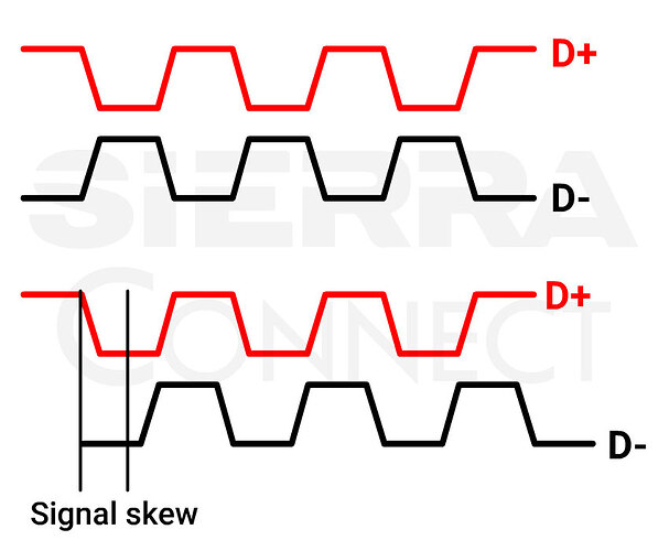
Signal skew is the timing mismatch or variation in propagation delay between multiple electrical signals that are intended to switch or arrive simultaneously at a destination.
This timing misalignment is a critical concern in high-speed parallel bus designs (like DDR memory, PCIe, or processor data paths) and clock distribution networks.
Types of signal skew:
-
Intra-pair skew: Timing mismatch between the two traces of a differential pair (e.g., USB D+ and D-).
-
Intra-bus skew: Timing variation between multiple signals within a parallel group (e.g., the 8 data lines of a byte lane).
-
Channel-to-channel skew: Timing difference between separate, independent links (e.g., between two PCIe lanes).
-
Clock-to-data skew: The misalignment between a data signal and the clock signal used to sample it.
Primary causes of signal skew with solutions
-
Long signal paths introduce greater propagation delay and are the most direct source of skew. Match trace lengths using serpentine routing to keep propagation delay consistent across all related nets.
-
Signals routed on different layers with different dielectric properties experience changes in effective Dk, which impacts propagation velocity. To counter this issue, keep high-speed signals on the same layer.
-
Unequal capacitive loading from vias, connectors, or component inputs increases the RC delay on some signals. To overcome this challenge, place vias symmetrically and maintain uniform capacitive loading across all signals within a bus or a differential pair.
