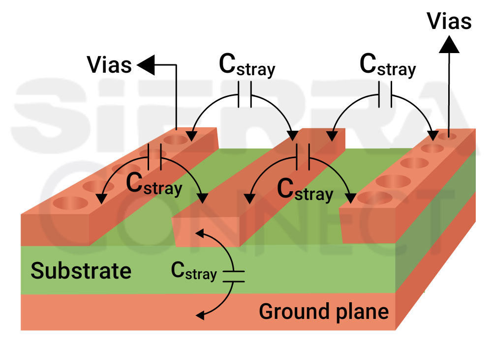
Parasitic capacitance (stray capacitance) is unintended capacitance that arises between conductive elements on a PCB due to their proximity and electric field coupling. This can degrade signal integrity, cause crosstalk, or introduce delays in high-speed circuits.
The parasitic capacitance is calculated using the formula C = (ε εoA)/d
Where,
ε= Dielectric constant of the material
εo =Permittivity of free space
A = Area of the plates
d = distance between the plates
Factors affecting parasitic capacitance:
- Trace geometry: Narrow spacing, wider traces, and proximity to reference planes increase capacitance.
- Dielectric material: Higher Dk values increase capacitance, and thinner substrates are more susceptible to coupling.
- Proximity to conductors: Closer signal lines, ground/power planes, or vias increase parasitic capacitance.
- Via structures: Stubs, through-hole, blind, or buried vias add capacitance between layers.
- Frequency: Shorter wavelengths make Parasitic capacitance more significant at higher frequencies.
To reduce parasitic capacitance, maintain optimum trace spacing, use low-Dk materials, and minimize via stubs.