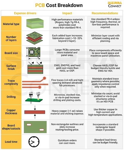
Designing a PCB isn’t only about achieving reliability. It’s also about balancing costs and manufacturability. Factors such as material type, number of layers, board size, drilling, and surface finish impact the overall budget.
In this infographic, we break down the key PCB cost drivers and a few decision-making tips that help you save money.
- Material type
The PCB laminate forms the foundation of your circuit and has a major impact on both cost and performance.
Standard FR-4 laminates are widely used for their balance in strength, cost, and insulation. However, high-performance materials like Rogers, polyimide, or high-Tg FR-4 offer superior thermal and electrical properties at a higher cost.
- Number of layers
Each additional copper layer increases fabrication cost by roughly 10–20% per layer beyond a basic two-layer board.
More layers mean additional lamination cycles, dielectric materials, and alignment steps.
For instance, a 6-layer board can cost almost twice as much as a 2-layer board of the same size.
Always minimize the layer count through efficient component placement and routing. Use power and ground planes strategically and consider alternatives like via stitching to reduce the need for extra layers.
- Board size
Board dimensions directly determine how much laminate and copper material your design consumes.
Larger boards require more raw material and reduce the number of boards that can fit on a fabrication panel, raising the cost per unit.
- Surface finish
The surface finish protects exposed copper and ensures reliable soldering. The finishes vary in cost, solderability, and shelf life.
Common finishes include:
- HASL (hot air solder leveling): Low cost, suitable for general use.
- OSP (organic solderability preservative): Environmentally friendly and cost-effective.
- ENIG (electroless nickel immersion gold): Excellent flatness and corrosion resistant, but more expensive.
- ENEPIG/hard gold: Used for wire bonding and edge connectors; expensive.
- Trace complexity
Trace width and spacing dictate the precision level required in imaging and etching processes. Finer geometries increase production difficulty, yield loss risk, and inspection time.
Traces below 4 mil spacing often require advanced etching and inspection equipment.
Increase tolerances whenever possible. Use standard 4–6 mil traces.
- Drilling
Drilling is one of the most cost-sensitive steps in PCB fabrication. The number, size, and type of vias, especially microvias and stacked vias, have a big impact on the overall cost.
Laser-drilled microvias, buried vias, or via-in-pad structures can increase costs by 30–50%, depending on layer count. Avoid stacked or blind/buried vias, if possible.
- Copper thickness
Thicker copper enhances current-carrying capacity and thermal performance but makes etching and lamination more challenging.
Doubling copper thickness from 1 oz to 2 oz can increase etching time and material costs by 20–40%.
Use heavy copper (≥2 oz) only in power or high-temperature regions. For signal layers, 1 oz copper is usually sufficient. You can also use selective plating to thicken copper only in specific areas.
- Board shape and cutouts
Non-standard outlines, slots, internal cutouts, and complex milling patterns require extra CNC machining and increase tool wear, which adds to the cost. Use rectangular board outlines whenever possible. Avoid excessive slots or cutouts unless they serve a mechanical purpose.
- Lead time
PCB fabrication costs depend on and turnaround time. Small or quick-turn orders need dedicated setups and higher priority, while larger batches spread setup costs across more boards, reducing the per-board price.
A quick-turn order can cost 2–3× more than a standard lead-time order.
Plan fabrication schedules in advance. Combine multiple designs in a single production batch to leverage panel pooling and lower per-board cost.
- Additional factors
While the above nine factors dominate cost, you can further optimize by considering these subtle options:
Solder mask color: Non-standard colors (black, blue, red) or glossy finishes can slightly increase cost compared to the default green.
Silkscreen printing: Double-sided or custom-color silkscreen increases setup cost.
Testing requirements: Flying probe or ICT testing adds to per-board cost but improves quality.
Tolerances: Overly tight dimensional or impedance tolerances demand precision processes, raising fabrication cost.
To design cost-efficient PCBs, always start with the manufacturer’s capabilities in mind. Review your fabricator’s standard design rules, such as minimum trace width, drill size, annular ring, and copper-to-edge clearance, before finalizing your layout. Using standard tolerances avoids custom tooling charges and reduces rejection rates.
For advanced boards like RF or high-speed designs, clearly indicate which rules are essential and which can be relaxed. This helps your fabricator focus on critical requirements without overcomplicating the board.
