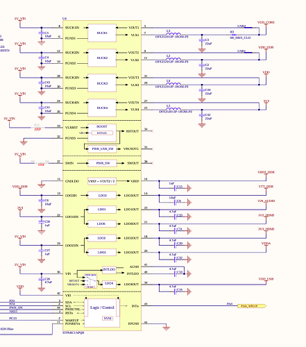
During the final review of my custom board schematic, I noticed something in the development board reference schematic that I had completely missed earlier — two labels: LNK1 and LNK2, connected to the PMIC outputs for VDD_CORE and VDD_DDR.
I didn’t include these in my design, and to be honest, I’m not sure what their exact purpose is.
Are they critical for functionality or testing? Is it okay to leave them out in a custom board?
custom board design
I’d really appreciate any insights or suggestions. just trying to make sure I haven’t overlooked something important.
LNK1 and LNK2 on the reference design exist as short circuits to link the VDD_CORE to a separate (but unnamed) net that brings the VDD_CORE voltage back to the PMIC. Likewise for VDD_DDR. The purpose of this is that there may be enough resistance in the PCB to cause a voltage drop because of current flow that would make the CORE see a voltage that is lower than it should be. By using the LNK1 and LNK2 it becomes easy to track the feedback voltage back from the MCU or DDR device. Thus the PMIC sees the lower than expected voltage and adjusts the output to compensate. So VDD_CORE is high as seen next to the PMIC, but it is right as seen at the MCU.
Does it matter? This cannot be answered without knowing what the voltages are, and what they’re meant to be. If the PMIC and MCU are in close proximity the risk is lower than if they’re far apart.
There may be some things you can do, but these come with a risk. Most PMICs are programmable, so you may be able to adjust the output voltage in the software and correct for the loss through the board. The risk is that if the MCU can operate at both a low current and also at a much higher current (say because you’ve changed between run and sleep modes, or you’ve altered the clock generation and now it is much faster) the change in current changes the voltage at the MCU. This means you must not program the new output voltage to exceed the highest allowed input voltage, or there is risk of damage to the MCU.
If the MCU programs the PMIC to the “correct” voltages after power up, the MCU is probably not running to its maximum potential, so the currents will be lower, and the voltage drop is lower and it works. When you change to the high performance state, you can measure the voltage drop on the supply voltage at the MCU and decide if it looks good enough, or if it needs to be raised. Just don’t raise it too far or the low power state might damage the MCU.
2 Likes
Thank you for the detailed explanation — it really helped clarify the purpose of LNK1 and LNK2. I just wanted to confirm: is adding a 0-ohm resistor sufficient for implementing them?
1 Like
A zero Ohms resistor is a common solution to this. The important thing is where it is located. It needs to be close to the place where the load is. In this case that means somewhere close to the MCU.
The principle is that the input impedance of the voltage feedback pin in high, so there is very little current in the feedback path. This means that the voltage loss due to the PCB resistance of the feedback path is negligible. Thus the resistive loss due to the resistance of the feedback path on your board can be neglected and you have the same voltage on the feedback pin as you have at the load. In this way any resistive loss in the high current path from the PMIC to the MCU is hidden because the sensing point is close to the load (the MCU) where the zero Ohms resistor is. This is referred to as “remote sensing” and is working in the same way as the remote sensing on lab power supplies.
2 Likes

