Non-symmetric Stackup

Hi all,

I’m working on an 8-layer PCB design for HSDD application and would like your input on the following stackup structure. Here’s the layer order from top to bottom:

  1. Signal
  2. GND
  3. PWR
  4. PWR
  5. GND
  6. Signal
  7. GND
  8. Signal

As you can see, the stackup is not symmetric, and it contains two adjacent power planes (which carry different voltages). GND and Signal layers are not fully mirrored either.

I’m particularly interested in hearing your thoughts on the advantages and disadvantages of this kind of stackup — especially any potential issues it might cause in terms of:

  • Signal integrity and return paths
  • Power distribution and decoupling effectiveness
  • Crosstalk or EMI
  • Manufacturing concerns like board warping due to asymmetry

This board carries some high-speed signals, so impedance and return path control are important to me.

Would love to hear your experiences or suggestions for improvements!

Thanks in advance.

1 Like

There’s a reason for rules in PCB design, but some of them can be disregarded if effort is applied to mitigate the problem(s) the rule was intended to prevent. This stack-up, if implemented correctly is one such example.

The critical part usually is that the board can warp during assembly. This happens because of a mismatch in the amount / position of copper on the relevant layers. If we make the assumption that PWR and GND layers will be close to 100% copper, then the mismatch here is layer 3 (PWR) and layer 6 (signal). So the question is whether we can make a signal layer look more like a plane, or a plane layer look more like a signal layer? Adding copper to the signal layer is not likely to be a big problem as long as it is connected to something sensible (like GND) and is well stitched in to the other GND planes. Depending on how much coverage on the signal layer can be achieved (which might not be as high as might be hoped), the next trick is to remove copper from the plane layer. This is easily done by turning it into a hashed plane. Tweak the size of the apertures in the grid to match the total coverage percentage on the signal layer and that should be fine.

Of course, the rest of the symmetry should be maintained in terms of the thicknesses of cores and prepregs.

It’s now time to consider the other matters. Let’s take return paths first. Every signal layer is adjacent to one or two GND layers (and nothing else is adjacent to them). This is a great start. Layer changes just require a GND plane stitching via(s) in the vicinity of the signal via and problem solved.

For the PWR layers, they are sandwiched between GND layers, but when you look at either of the PWR layers, each PWR layer references both a GND layer and the other PWR layer. Therefore some signal flow will be induced by PWR-L3 in PWR-L4, and vice-versa. This is crosstalk between PWR layers and is not desireable. However, it is easy to do something to minimise this. If the spacing between L2 (GND) and L3 (PWR) is made small relative to the spacing between L3 (PWR) and L4 (PWR), it follows that the bulk of the coupling will be between PWR and GND, and much less between PWR and PWR.

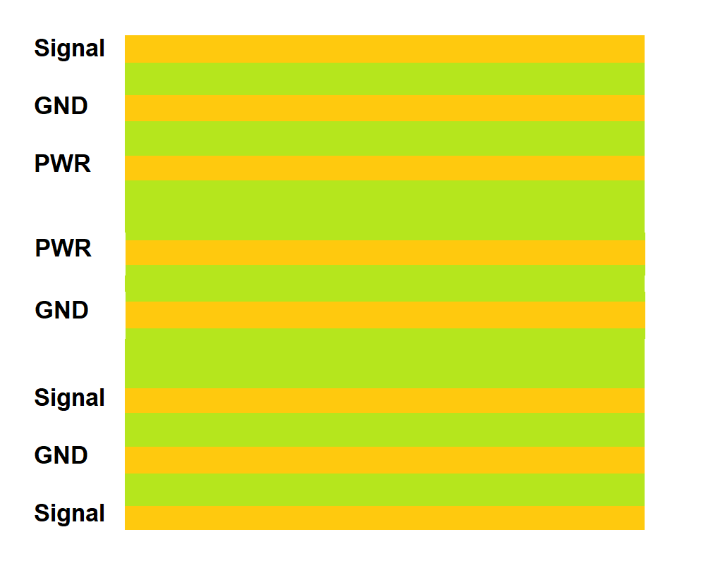
If this is the case, then by symmetry, the spacing between L6 (Signal) and L7 (GND) must also be small. This is good if this is a high signal density design because it means that thin traces will probably give sensible impedances allowing for high routing density. If these traces are thin, then having fairly thin traces on the outer layer makes sense, and this points to making the spacing between L1 (signal) and L2 (GND) also be narrow (and likewise L7 (GND) to L8 (signal). So it appears that the stackup to aim for should have these thicknesses:

L1-L2 = narrow

L2-L3 = narrow

L3-L4 = wide

L4-L5 = narrow

L5-L6 = wide

L6-L7 = narrow

L7-L8 = narrow

This should ensure that return paths are as close to ideal as is reasonably possible. GND vias are all that are needed to provide the return paths for all signals. Power crosstalk is minimised by distance (reduce coupling). Signal crosstalk is no different to how it would be if you added more GND layers. As a consequence, the EMI should be minimal. It seems like the manufacturability should be good. It is a little bit unusual so the PCB price may not be as cheap as other 8-layer boards, but it doesn’t look as though it should cost too much. The only other thing worth adding is that if L3 (PWR) is now a perforated layer to match the percentage copper weight of L6 (signal) the reduction in the amount of copper on L3 suggests putting the lower current supplies on this layer if possible.

In principle, this asymmetric layer stack looks as though it is a sound engineering solution. The only other remark is to verify with your PCB house that they can make it without any serious issues.

4 Likes

Thanks Jon!!!

Very thorough explanation. Thanks.

1 Like

In addition to Jonathan’s great response about the mechanical aspects and return path aspects of this stackup choice, I have a few other things to consider on as well.

When attempting to decide whether to place PWR layers higher or lower in the stackup, there are a couple of things to consider. High speed signals require bursts of power to prevent momentary slumps in the power nets. Bypass capactitors aid IC pins momentray demands, and the main power supply backfeeds those caps although at a slower pace (and generally at greater distance through board). So consider which mounting side the high consumption ICs are placed in relation to their bypass caps side placement. If the ICs and bypass caps are on the top side, then PWR feed layers benefit from being closer to those components. If the bypass caps are on the bottom side and directly under top side ICs, then PWR layers may work better lower in the stackup. Remember that the caps fill in the differences of demands (fast) and supply (slow). If the slower power supply cannot resupply the caps fast enough, then the cap loses it ability to keep up with the IC repeated power requests.

Now lets consider the signals themselves. High speed signals can experience degradation due to via stub lengths and signal connection layers stackup position can determine via stubs lengths. So where connecting layers are in the stackup and whether the design is using blind or buried vias can have some effect on how stable the signal will be. I will say that many designs likely do not have to worry too much about stubs but if signal speeds make this a concern, then that should be balanced into stackup considerations.

3 Likes

Reviewing the inital stackup, lets make an example assumption about the circuit for a moment. Lets assume this is for a DDRx type of circuit with high speed MCU and memory are on top layer. In this case we most likely will want high speed signal paths short as possible and benefits from using a common L2 GND for both HS signal layers. In this case, we might choose the stackup to look like this:

L1 HS Signal and HS components

L2 GND

L3 HS Signal

L4 GND

L5 PWR

L6 PWR and/or LS signal

L7 GND

L8 LS Signal, LS components, bypass caps

3 Likes

I would use a symmetric stack to avoid manufacturing issues.

I recently designed an 8 layer board with quite similar requirements and the stack was:

Top.. Signal.

  1. Ground plane.
  2. Power plane. (split).
  3. Signal.
  4. Signal.
  5. Power plane.
  6. Ground plane.
  7. Signal.

For controlled impedance I always ask my vendor for track, track and gap and interlayer spacing and materials. They are in the business of making them and I use their expertise to guide me (note that no two fabricators will give the same answers so choose your vendor wisely).

My signal speeds are up to 5Gb/s (PCIe gen 2) and there are actually 4 independent impedance rules.

I normally run the highest speed signals (especially differential pairs) on the surface due to lower dielectric losses and the fact that surface tracks are typically a bit wider than internal for a given impedance which gives more margin for slight over or under etch.

2 Likes