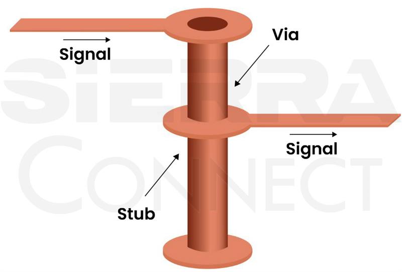
A via stub is the unused, plated portion of a via barrel that extends beyond the signal layers it is intended to connect. The unused segment behaves like an open-circuited transmission-line stub, introducing reflections, increased capacitance, and insertion loss.
The reflections caused by the stub can interfere constructively or destructively with the main signal, leading to data errors or reduced eye opening. As a PCB designer, you should aim to eliminate via stubs to maintain signal integrity.
Quick tips to minimize via stubs
- Use blind or buried vias to avoid long stubs.
- Implement vias-in-pad and fill them to shorten stubs.
- Use staggered microvias instead of stacked ones.
- Remove non-functional pads and enlarge antipads in padstacks.
- Ask your fabricator to back-drill via stubs. Specify back-drill details on the fab drawing.